Results
Camera Configuration
The initial camera configuration over SCCB is verfified using the MCU, by reading the registers that were set to achieve QVGA and YUV configuration and also various autoexposure settings, these register writes were verfied by printing over the UART using debug terminal. This ensured that we had correctly configured the camera using the MCU to be able to read out data onto the FPGA for bitmasking.
Pixel Capture by FPPA and Bitmasking, and Frame Data storage signals
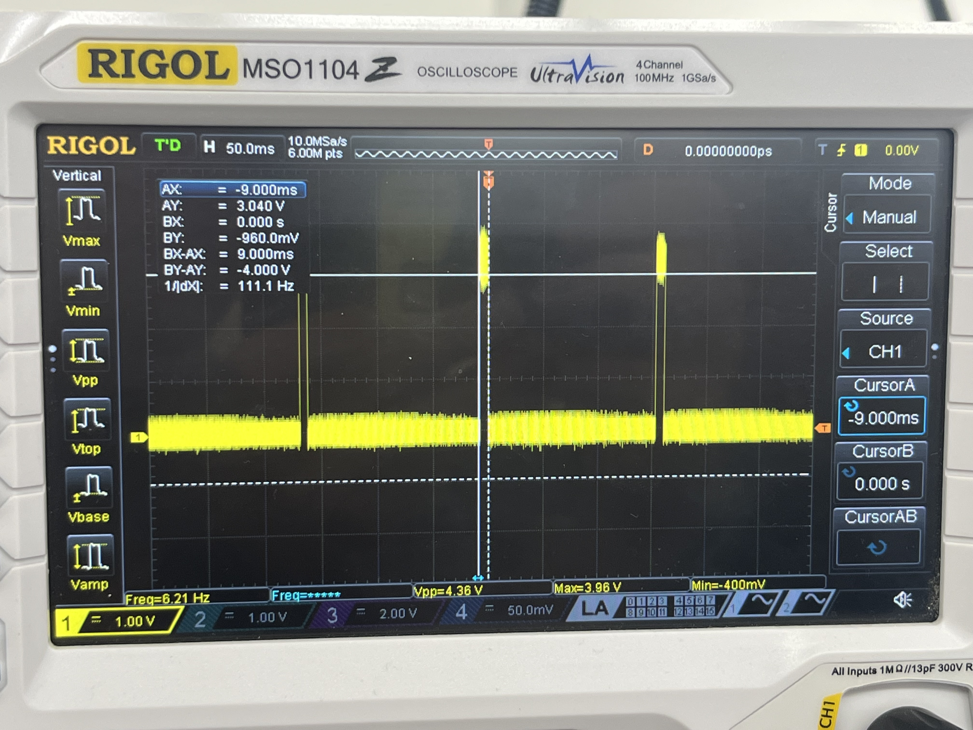
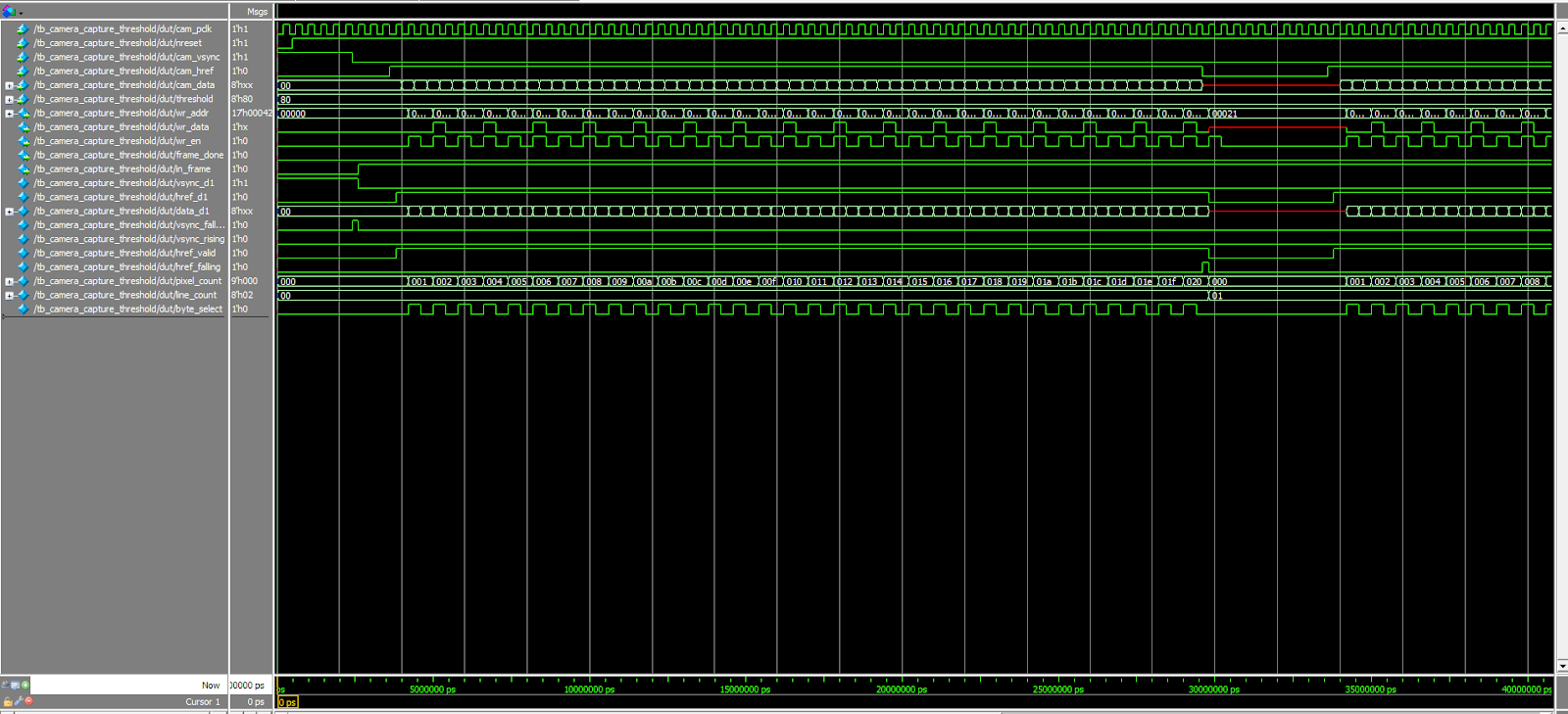
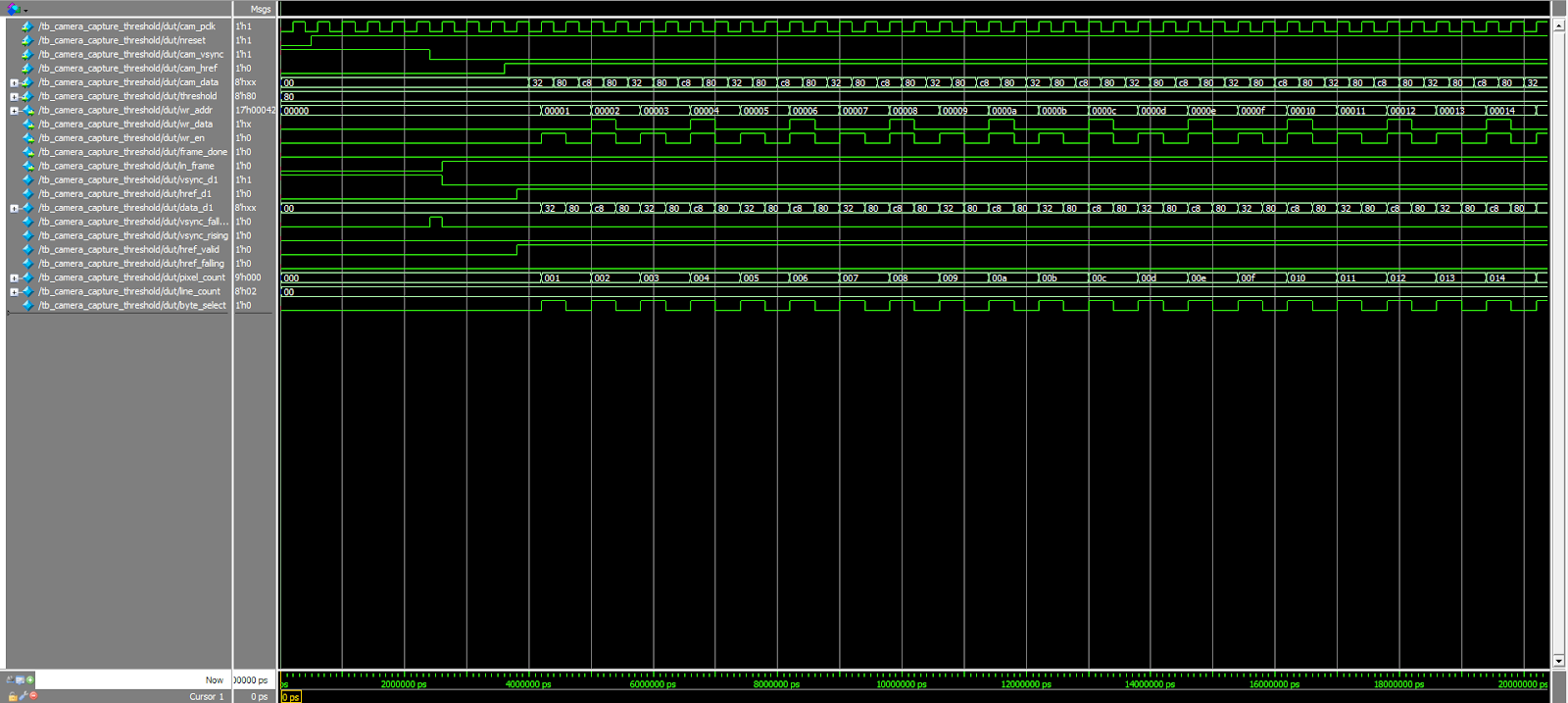
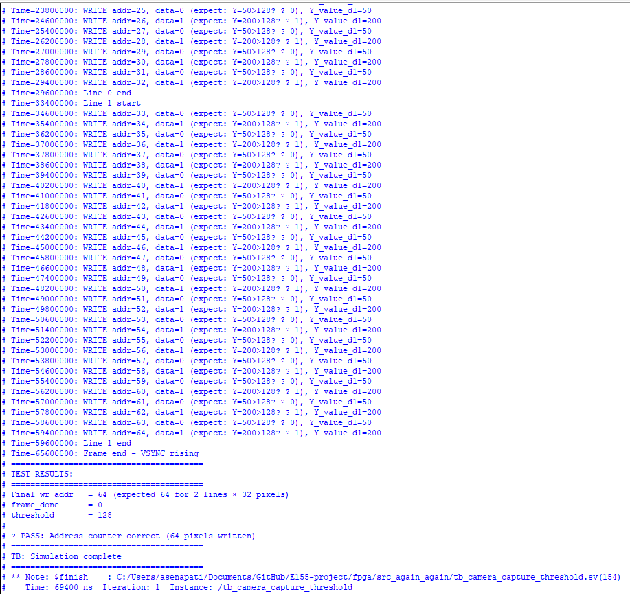
The FPGA had camera_capture_threshold module that captured the images, and bitmasked based on threshold specified, and simulataneously wrote out the pixel bits, these signals were read into the other module and saved on the dual frame buffer. This bitmaksing of images, and the correct capture of all the frame data at the appropriate frame rate was verfied using oscilloscope, where the intermediate fpga signals from this module were mapped to digital pins, and visualized on oscilloscope, and we saw exactly all the 76800 pixels being bitmasked in the pclk domain, and full frame being captured simulataneously, and write address and enable signals being properly triggered to store this bitmasked image. This process was also verified through testbenches which confirmed that correct signal were being asserted. This was verified with the fact that we obsevred the same frame rate of 6 FPS, as outputted by the camera, being read out by FPGA.

SPRAM Frame Buffer, Bitmasked frame transfer, and Line Detection
The SPRAM frame buffer and bitmasked image transfer over SPI was initially verified over Logic Analyzer to ensure SPI communication worked properly, and then also this was confirmed as the MCU was able to read in all these pixel data, and print the number pixels it received, and print the entire frame over the debug terminal, and by place different objects/lighting conditions in front of camera, and observing the desired results, we were able to verify and test that FPGA was able to store and communicate the bitmasked pixels over SPI correctly. This itself was also sufficient for us to verify that line detection was possible as we verified it by placing white and black paper, and counting the total number of the black and white pixels being observed in a frame, and toggling a GPIO based on if the number of black/white pixels fell in a certain range, confirming with our visual input, we ensured that this worked appropriately. We also verified that the FPGA was sending frames at 6 fps to the camera, which can be seen in the scope trace below, where we captured the FPGA’s frame_ready signal.