FPGA Overview
General Overview
The project uses two FPGAs, each of which is independent from the other. The FPGA’s purpose is to capture the raw pixel data in YUV422 QVGA format from the OV7670 camera, and then store the bitmasked frame of Y-values of pixel data based on a pre-determined threshold by the user. This bitmasked image is stored in SPRAM frame buffer in the FPGA, before being sent to the MCU over SPI.
System Architecture:
OV7670 Camera → Threshold Module → Frame Buffer → Serial Interface → MCU
(YUV422 QVGA) (Y-only, 1-bit/pixel)  (SPRAM)         (SPI)
RTL Block Diagram
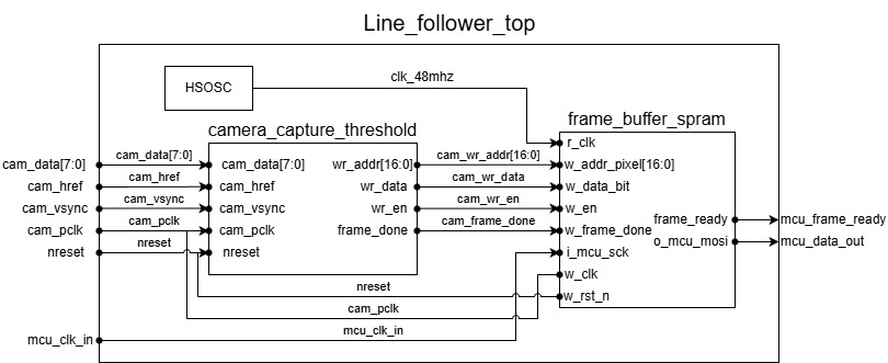
The block diagram describing our RTL, which can be seen below.
OV7670 Camera Pixel Capture and Bitmasking
YUV422 Format and Y-value (luminosity) of pixel extraction
The OV7670 camera supports sending data in multiple formats, but for our project, as we realized we only care about differentiating between two colours of the lines and the track, we could easily do this by using YUV format output, and just using the Y values of the pixel data which represent the luminosity, while ignoring the U/V values which encode the chroma/colour data. Given we chose black line on white background for our testing purposes, using Y values would be sufficient, as they would have different intensity levels.
YUV422 Data Format:
The YUV data sent by the camera is in the format of 8-bit Y, 8-bit U or 8-bit Y, 8-bit V, therefore, we only care about every other byte of pixel data which represent the Y values for all the 76,800 pixels we receive in the QVGA format.
Data Stream:     Y0  U0  Y1  V0  Y2  U1  Y3  V1 ...
Bytes Captured:  Y0  --  Y1  --  Y2  --  Y3  -- ...
This also helps us save lot of memory as we reduce the frame data by 94%
- Full YUV422: 76,800 pixels × 2 bytes = 153,600 bytes
- Y-only binary: 76,800 pixels × 1 bit = 9,600 bytes
Threshold Module Operation
The camera_capture_threshold module runs entirely in the camera pixel clock domain and processes incoming YUV422 data in real-time.
Key Signals:
// Inputs
cam_pclk:   Pixel clock from OV7670
cam_vsync:  Frame sync (LOW = active frame)
cam_href:   Line valid (HIGH = pixel data valid)
cam_data:   8-bit YUV422 data bus
threshold:  8-bit comparison value (our chosen value 141)

// Outputs
wr_addr:    17-bit pixel address (0-76,799)
wr_data:    1-bit thresholded result (bright/dark)
wr_en:      Write enable pulse
frame_done: Frame complete pulse
Operation:
The module uses a priority-based control structure with four operations:
- Frame Start (VSYNC falling edge) - Reset counters, begin capture
- Frame End (VSYNC rising edge) - Signal completion
- Pixel Capture (during frame with HREF valid) - Threshold and write Y bytes
- End of Line (HREF falling edge) - Reset line counters
Byte Selection Logic:
A simple toggle mechanism parses the YUV422 stream:
if (byte_select == 0) begin      // Y byte
    wr_en   <= 1;
    wr_data <= (data > threshold);
    byte_select <= 1;            // Next is U/V
end else begin
    byte_select <= 0;            // Skip U/V, next is Y
end
This alternates between capturing Y bytes (luminance) and skipping U/V bytes (chroma).
SPRAM Frame Buffer and SPI Transfer
Memory Architecture
The iCE40 UP5K provides 128 KB of SPRAM (Single-Port RAM), which we use for double-buffered frame storage:
- Each frame: 76,800 bits = 4,800 words (16 bits/word)
- Bank 0: Addresses 0x0000-0x12BF
- Bank 1: Addresses 0x1300-0x257F
- Total usage: 9,600 words (15% of SPRAM capacity)
Bit Packing
Since the threshold module outputs 1 bit per pixel, data is packed into 16-bit words:
Pixel Address [16:0]:
  Bits [16:4] → Word address (0-4,799)
  Bits [3:0]  → Bit position (0-15)
When 16 bits accumulate in the camera domain, they’re latched and transferred to the system clock domain (48 MHz) for SPRAM write.
Double Buffering (Ping-Pong)
The frame buffer uses ping-pong buffering to enable simultaneous camera write and MCU read:
- Camera writes to Bank A, MCU reads from Bank B
- On frame completion, banks swap roles
- Camera immediately starts writing to Bank B
- MCU continues reading completed Bank A
- Process repeats continuously
This ensures no frame drops at 6 fps, even if the MCU lags behind by one frame.
Clock Domain Crossing (CDC)
The system operates across two asynchronous clock domains:
- Camera domain: 2.5 MHz (from OV7670)
- System domain: 48 MHz (internal oscillator)
All cross-domain signals use 3-stage synchronizers to prevent metastability.
Data is latched in the source domain before the control signal toggles, ensuring stability during crossing.
Serial Interface to MCU
The FPGA implements a SPI slave interface:
Protocol:
- FPGA asserts frame_ready when new frame available
- MCU generates SCK pulses (3-48 MHz recommended)
- FPGA outputs one bit per SCK falling edge
- After 76,800 bits, FPGA deasserts frame_ready
The module uses priority-based logic:
- New frame event - Reset address, load first word from SPRAM
- Load complete - Capture SPRAM data into shift register
- Shift on MCU clock - Output bits serially, fetch next word when needed
Timing:
At 10 MHz SCK: 76,800 bits / 10 MHz = 7.68 ms per frame
Camera frame period: 9ms ms per frame( at 6 fps)
Pin Count
- Camera interface: 11 pins (pclk, vsync, href, data[7:0])
- MCU interface: 3 pins (sck, mosi, frame_ready)
- System: 1 pin (reset)
- Total: 14 I/O pins
Performance Summary
Camera Capture:
- Frame rate: 6 fps
- Pixel rate: .46 Mpixels/sec
- Bit rate: .46 Mbits/sec (after thresholding)
Testing Results
The system has been validated with:
- Testbench to verify the module
- Continuous frame capture at QVGA resolution
- Correct YUV422 byte selection (Y-only)
- Threshold discrimination (black line detection)
- Bank swapping without corruption
- Proper Serial readout over SPI
The hardware has been tested extensively and performs reliably in the line-following application.